Diy-CAD
Contents
- 1 Workshops
- 1.1 GAPS | ɖǟռɢɖʊȶ ₣ⱤØ₥ ⱧɆⱠⱠ | gambar pisibi-mu sendiri - Creative PCB-design Workshop, Ruang MES56, Oktober 2022
- 1.2 GAPS | gambar pisibi-mu sendiri - Creative PCB-design Workshop, Gudskul, September 2022
- 1.3 GAPS - Creative PCB-design Workshop, Electronic Wonderland August 2022
- 1.4 GAPS (GaPiSen) | gambar pisibi-mu sendiri - Creative PCB-design Workshop with Diy-CAD, Lifepatch 30. June 2022
- 1.5 Workshop at GOSH2017, Santiago de Chile
- 2 diy-CAD Description
- 2.1 Prepare 400% scaled, printed, laminated and cut-out smd parts.
- 2.2 Information about these parts
- 2.3 Experience from the first workshop at Dimension Plus LAB, TW
- 2.3.1 Discuss the difference between the "schematic" representation and "physical" implementation
- 2.3.2 Start layouting and drafting the correct connections with pencil
- 2.3.3 Overlay with a transparency sheet and draw the circuit traces and pads
- 2.3.4 Scan (or photo), scale it back down, print and etch the boards
- 2.3.5 Etch the boards or send it for manufacturing
- 2.4 Workshop at GOSH2017, Santiago de Chile
- 2.5 Workshop at Take-Space, Fablab Hamamatsu, Japan
- 2.6 Reflections
Workshops
<<- Back to ROŠA - Regional Open Science Hardware & Art, Indonesia

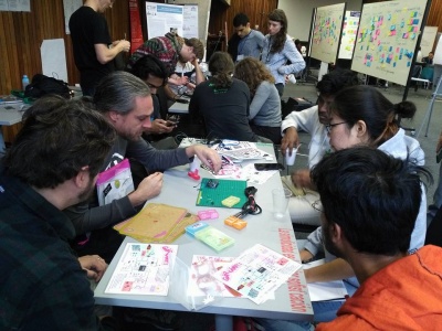
GAPS | ɖǟռɢɖʊȶ ₣ⱤØ₥ ⱧɆⱠⱠ | gambar pisibi-mu sendiri - Creative PCB-design Workshop, Ruang MES56, Oktober 2022

Para sobat kreatif, desainer, pelukis pintu terbuka lebar! Pengetahuan mengenai elektronik dan desain sirkuit tidak diperlukan.
Tangal: Thursday, 20. October, starting at 17.00. Duration 2-3 hours and open end jam & nongkrong. Snacks and drinks will be provided, feel free to bring something too!
Jam: 5 Sore - Selesai
Lokasi: Ruang MES56, Jl. Mangkuyudan No.53 A, Mantrijeron, Kota Yogyakarta, 55143
Sebagai sebuah lokakarya desain/menggambar kreatif, kami ingin menjelajahi bagaimana pengetahuan dapat digunakan untuk menciptakan desain-desain unik dari sirkuit-sirkuit elektronik yang fungsional. Kami juga ingin membahas makna Open Hardware dan mengapa membagi instruksi yang detil dapat menjurus kepada sebuah keberagaman desain dan memperbesar aksesibilitas dalam lokakarya-lokakarya elektronik DIY.
Di dalam lokakarya menggambar kreatif, kita akan mempelajari pengenalan paling dasar bagaimana membaca skema sirkuit-sirkuit elektronik, dan bagaimana menerapkannya sebagai sebuah PCB yang fungsional di mana seluruh sambungan tergambar di atas tembaga. Kita akan mempelajari apa yang dimaksud dengan jejak kaki komponen dan apa yang dimaksud dengan “lapisan-lapisan” berbeda dalam menyiapkan sebuah desain PCB sebelum di produksi (di pabrik-pabrik di Cina untuk keperluan etsa rumahan) .
Lokakarya ini juga akan berperan dalam usaha untuk memikirkan ulang metodologi diy-CAD (do-it-yourself Children Aided Design) dan mengaplikasikannya pada Noise Touch Synthesizer, berbasis sirkuit amplifier LM386
Bagaimana sirkuit beroperasi?
Sirkuit contoh tersebut berbasis LM386, sirkuit amplifier 1W sederhana dan ia dapat digunakan untuk membuat desain touch noise synthesizer Anda sendiri!! Alat ini dapat bekerja sebagai sebuah amp distorsi bagi bunyi input Anda (seperti ɖǟռɢɖʊȶ), yang nantinya anda dapat *** dan menciptakan bunyi noise dan drone dari neraka. Dan alat ini menggunakan LED pink!
Seluruh material akan tersedia di laman daring, termasuk bolpen dan kertas, spidol dan footprints.
Creatives, designers, painters welcome! No previous knowledge in electronics or circuit design is needed.
As a creative design / drawing workshop we want to explore how creativity can be use to make unique designs of fuctional electronic circuits. We also will discuss what means Open Hardware and why sharing detailed instructions can lead to a diversity of personal designs and improving the accessibility for DIY electronics workshops.
In this creative drawing workshop, we will learn the most basic introduction to read schematics of electronics circuits, and how to implement it as a functional PCB (Printer Circuit Board) where all the connections are drawn in copper. We will learn what are footprints of components and what are the different "layers" for preparing a PCB design for manufacturing (in China factory of DIY home etching).
This workshop also serves for re-thinking the diy-CAD methodology (do-it-yourself Children Aided Design) and applying it to Noise Touch Synthesizer, based on the LM386 Amplifier circuit.
What circuit will we do?
The example circuit is based on the LM386, simple 1W amplifier circiut and it can be used to make your own design of a touch noise synthesizer!! The device can act as a distortion amp for your input sound (such as ɖǟռɢɖʊȶ), which you can then f*.%-up and create noise and drone sounds from ⱧɆⱠⱠ. And it has a pink LED on it!
All the materials will be available on site, pen and paper, colors, footprints.
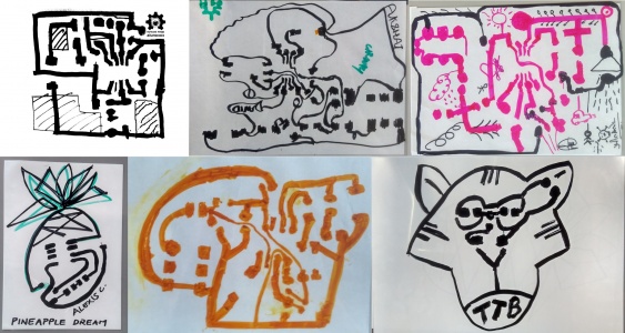
Examples of beautifully creative Touch Interfaces on PCB material Contoh-contoh Antarmuka Sentuh yang apik di atas material PCB:


This workshop is part of ROŠA - Regional Open Science Hardware & Art, Indonesia, a regional event series combining longer on-site group residency, aswell as a research & production lab, local outreach and a gathering of interesting players from the region of South East Asia. Supported by the GOSH regional events grant via Sloan Foundation)
GAPS | gambar pisibi-mu sendiri - Creative PCB-design Workshop, Gudskul, September 2022

Tangal: Monday, 26. September, starting at 15.00. Duration 2-3 hours and open end jam & nongkrong. Snacks will be provided, feel free to bring something too!
Jam: 3 Sore - Selesai
Lokasi: @ Gudskul, Jagakarsa, Jakarta Selatan
Jl. Durian No. 30A, RT.4 / RW.4, Jagakarsa, Kec. Jagakarsa, Kota Jakarta Selatan, Jakarta 12620
Registrasi: https://forms.gle/xRUVC9jPitv4vWCGA

Terima kasih to our hosts at gudskul!
Siapapun yang tertarik dapat mengikuti ini, tidak memerlukan pengetahuan dalam dunia elektroni maupun desain sirkuit.
Sebagai kegiatan pembelajaran. kami mau menjelajahi bagaimana kreativitas bisa digunakan untuk membuat desain sirkuit elektronik yang unik. Kita juga akan berdiskusi soal Open Hardware dan kenapa membagi instruksi yang terperinci dapat membawa desain sirkuit yang beragam dan mampu memperbaharui aksesibilitas yang baru untuk DIY Workshop Elektronik.
Impressions


Creatives, designers, painters welcome! No previous knowledge in electronics or circuit design is needed.
As a creative design / drawing workshop we want to explore how creativity can be use to make unique designs of fuctional electronic circuits. We also will discuss what means Open Hardware and why sharing detailed instructions can lead to a diversity of personal designs and improving the accessibility for DIY electronics workshops.
In this creative drawing workshop, we will learn the most basic introduction to read schematics of electronics circuits, and how to implement it as a functional PCB (Printer Circuit Board) where all the connections are drawn in copper. We will learn what are footprints of components and what are the different "layers" for preparing a PCB design for manufacturing (in China factory of DIY home etching).
This workshop also serves for re-thinking the diy-CAD methodology (do-it-yourself Children Aided Design) and applying it to the fork of the peepsy, based on the Continuity Tester by David Johnson-Davies. The peepsy circuit is based on the ATTINY85 functions as a continuity tester, the famouse "peeps" of every multimeter, that allows you to test if an electric connection is present, testing your aux cables, or debbugging other electronics. And it has a pink LED on it!
What circuit will we do?
The example circuit is based on the peepsy, by Michael Egger (a.n.y.m.a.) and it has even a practical function as a continuity tester, the most useful tool to test if a connection is present, in a cable or on a circuit. It's the "peep" that is one of the functions of all multimeters, and usually the one we use the most! The circuit is very simple, 1 capacitor, 2 resistors, 1 LED, a buzzer to make the "beep", a coin battery holder and an µ-controller (the Attiny85). Due to the special software on the attiny, it will "sleep" all the time, and only use a little electricity when testing, so the battery last almost forever!
All the materials will be available on site, pen and paper, colors, footprints.
GAPS - Creative PCB-design Workshop, Electronic Wonderland August 2022


The laminates to cut and MASK for etching are available on the peepsy github.


GAPS (GaPiSen) | gambar pisibi-mu sendiri - Creative PCB-design Workshop with Diy-CAD, Lifepatch 30. June 2022
<<- Back to ROŠA - Regional Open Science Hardware & Art, Indonesia#Preparatory_Activities
Schedule: Thursday, 30. June, starting at 17:30. Duration 2-3 hours. Snacks will be provided, feel free to bring something too!
Location: @ Rumah lifepatch, Yogyakarta
Re-thinking the diy-CAD methodology (do-it-yourself Children Aided Design) and applying it to the fork of the peepsy.
In this creative drawing workshop, we will learn the most basic introduction to read schematics of electronics circuits, and how to implement it as a functional PCB (Printer Circuit Board) where all the connections are drawn in copper. We will learn what are footprints of components and what are the different "layers" for preparing a PCB design for manufacturing (in China factory of DIY home etching).
As a creative design / drawing workshop we want to explore how creativity can be use to make unique designs of fuctional electronic circuits. We also will discuss what means Open Hardware and why sharing design instructions can lead to a diversity of personal designs and improving the accessibility for DIY electronics workshops. No previous knowledge is needed to participate successfully!!


All the materials will be available on site, pen and paper, colors, footprints.
What circuit will we do?
The example circuit is based on the peepsy, by Michael Egger (a.n.y.m.a.) and it has even a practical function as a continuity tester, the most useful tool to test if a connection is present, in a cable or on a circuit. It's the "peep" that is one of the functions of all multimeters, and usually the one we use the most! The circuit is very simple, 1 capacitor, 2 resistors, 1 LED, a buzzer to make the "beep", a coin battery holder and an µ-controller (the Attiny85). Due to the special software on the attiny, it will "sleep" all the time, and only use a little electricity when testing, so the battery last almost forever!
How was it?

Workshop at GOSH2017, Santiago de Chile
300px


See discussion on GOSH Forum.
diy-CAD Description
We have been developing and testing the new workshop for GOSH2017, called diy-CAD (do-it-yourself Children Aided Design), specifically for the Gär Lämpli project (fermentation lamp). The core idea of the workshop-kit is tool for creative designs of printed circuit boards, introducing basic concepts of Open Hardware being something to re-design for your own use. Going from an open/shared schematic and bill of materials to a manufacturable board, using SMD (surface mount devices) components. The design tool is mostly pen and paper, where the footprint of the parts are scaled 400% and can be freely rearranged, and then a copper layer can be painted to draw the functional board design by hand. This was the first time the kit was tested and i am very thankful for feedback if this is useful at all, or other uses of it.
說明: DIY 兒童輔助設計電路(DIY-CAD,do-it-yourself Children Aided Design) 是馬克(Marc Dusseiller Dusjagr)為發酵小燈Gär Lämpli 專案設計,也為了2017年的"開放科學硬體大會"The Gathering for Open Science Hardware (GOSH)發展與測試的DIY兒童輔助設計工具。主要核心概念以創意設計的列印電路紙板為工具,藉此讓大家認識開放硬體的基本概念,即利用已經開放的事物依自己所需重新設計,從開放/分享的工程圖與一堆材料中,SMD的電子元件,完成可製造的電路板設計。 主要的工具是紙跟筆,工具中的電子材料紙元件都已經被放大400%,元件相連接的電路可以用手自由地創造塗繪,這套工具還在測試當中,如果有人使用或是受益,馬克將會非常感謝您的回饋。
Prepare 400% scaled, printed, laminated and cut-out smd parts.
放大400% 的smd元件,列印,護貝,剪下,備用


Download the files from the github.
下載可列印smd元件圖案 github.
Information about these parts
coming soon...
Experience from the first workshop at Dimension Plus LAB, TW
首次工作坊實驗測試於台灣LAB By Dimension Plus!
Discuss the difference between the "schematic" representation and "physical" implementation
討論示意圖中符號的代表意義與實體物件的整合


Start layouting and drafting the correct connections with pencil
開始用鉛筆畫出正確的連接配置與草稿


we should add some sticky tape to fix them...
建議在smd紙元件的背後加上膠帶或黏土方便固定...
Overlay with a transparency sheet and draw the circuit traces and pads
放上透明膠片,描繪鉛筆的電路與元件連接點
Make sure you take some photo of your layout to refer to the part's position later.
記得幫你排好的元件位置拍照,以免元件不小心挪動位置。


Scan (or photo), scale it back down, print and etch the boards
掃描或拍照,縮小,列印,蝕刻電路板
Take a decent photo, check for reflections from lamps and stuff. Edit the photo in GIMP, to select all surrounding areas and invert the selection. Fill with FG (black), copy, create from clipboard -> new file. import in Inkscape, rescale to original size (some markings on the drawing would be great). Last edits can also be done in inkscape, like adding logos, version numbers, open source coconuts or defined drill holes, cut-layer etc...
如果使用拍照,注意膠片上的反光等,在GIMP影像處理軟體中,全選>反轉選取,填入黑色前景,複製。然後在Inkscape程式,新增一個檔案,從剪貼簿中貼過來之前複製的圖,改變尺寸至原來尺寸,在Inkscape做最後微調,例如增加logo,版本,開源椰子計畫或預計開孔位置,電路層等。


Etch the boards or send it for manufacturing
蝕刻電路板或送至工廠製作
Panel, Print and etch, or use pdf2gerber to send it for manufacturing. A version was imported to kiCAD and Gerber files produced. You can find it on kitnic.
板子,列印與蝕刻或使用pdf2gerber轉檔,送至工廠製作。
新版可輸入至kiCAD,製作出Gerber檔案,你可在此找到。
kitnic.


Workshop at GOSH2017, Santiago de Chile
300px
See discussion on GOSH Forum.
Workshop at Take-Space, Fablab Hamamatsu, Japan
Designing and making the boards
Impressions from the diy-CAD creative PCB design workshop in Take-Space / Fabalab Hamamatsu


Preparing the files for Manufacturing

Selected Take's Unagi Version of the GärLämpli (and thx to Nozomi for nice calligraphy!!) and prepared the file in Inkscape to get extra features and make Shenzhen Ready for manufacturing. See a how to here.
Uploaded the Gerber file and bom to another Github and shared in Kitnic.it
Making a Kit
See more about the Gär Lämpli and the Unagi.

... and even a nice little box.


Reflections
I hope more people are picking up the diy-CAD design tool, or also just the kits we developed using it. I think it can have it's special role in education (not as a starting point), fun for geeks/adults, aswell as complete newbies to open hardware & pcb design. The full process gives them an amazing experience from drawing and having first time a pcb made in their hands in one (long) day.
This educational workshop project, specifically with attiny85 audio prog bootloader, is maybe not the most suitable, if its just about creative pcb making, other sound toys, synths and blinke-shit might do the trick. But then on the other side, the audio programmable attiny, also called CocoNEO, is a very powerful low-cost µ-controller science/toy with much broader possible applications, similar to other data-loggers available by publiclab and many others.