Elektrowetting
Contents
Introduction
- Electrical charge of the surface changes the shape of water drops (before 1875)
- Electrowetting is the modification of the wetting properties of a surface by applying different electric fields (1981)
- "fluid transistor" for manipulating chemical and biological fluids (1980)
- Electrowetting on this dielectric-coated surface, EWOD (1993)
- Digital Microfluidic Circuits
What you need:
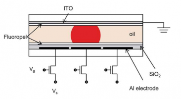
- insulating dielectric and hydrophobic layers
- immiscible fluids
- DC or RF power
- mass arrays of miniature interleaved electrodes (Indium tin oxide (ITO))
- digital control
- nano droplets
What you can do:
- move droplets in linear, circular and directed paths
- pump fluids
- mix fluids
- fill reservoirs
- move droplets over sensors or heaters
- control fluid flow electronically or optically
source: http://en.wikipedia.org/wiki/Electrowetting
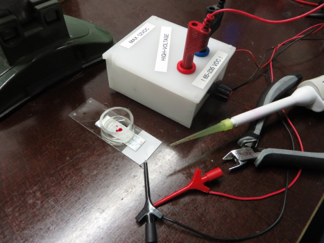
DIY experiment
What you need:
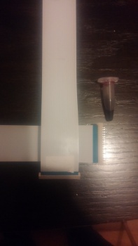
- ribbon cable
- water, oil
- high voltage (how high? Amperage? will 80v do?)
What you can do:
DIY Designs
Fluxology
FluxMux-Device
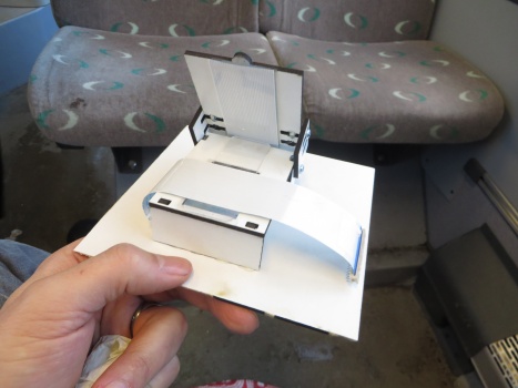
Based on two crosswise flat ribbon cable the FluxMux device is an easy way to create a digital microfluidic device. An array of power leds shines through the grid to make drops visible.
The control is multiplexed.
Flux Technologies
comming soon...
Bio Device
Surface Coating
Electronic Control
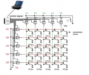
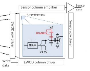
[1,2,3]
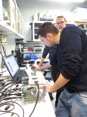
Visit to DropBot @ Helsinki University
== DigiFlux Shield ==file:///media/gaudi/CANON_DC/DCIM/124___03/IMG_7383.JPG
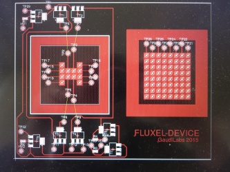
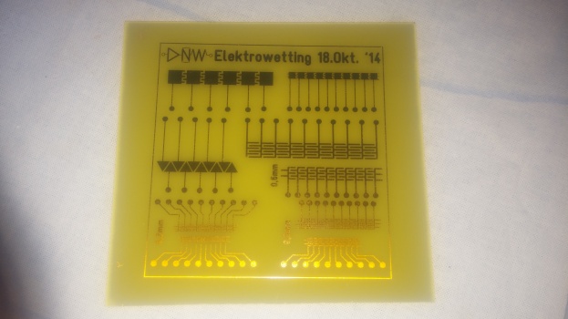
Layouting first prototype of DigiFlux with array of fluxels
Etching some prototype shields.
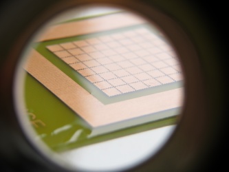
Spin-coating with PDMS and teflon
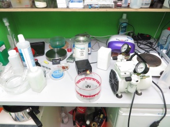
Intense fluxing (hacking session)
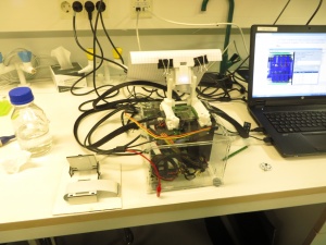
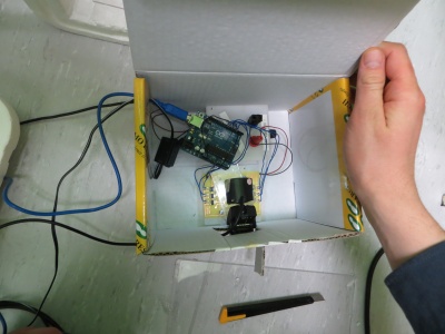
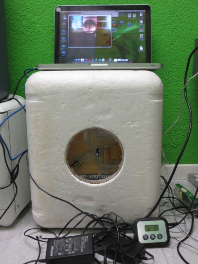
Embedding the fluxel device in a fancy German box
File:fluxel incubated.JPG
Incubating cells on the fluxel device
References
Fast Fabricating Electrowetting
Low Cost PCB Digital Microfluidic
Videos
On chip Sample preparation utilising EWOD Concept
DNA Lab on a Chip
Sandia Digital Microfluidic Hub
The Electrowetting Display
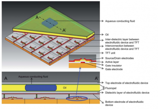
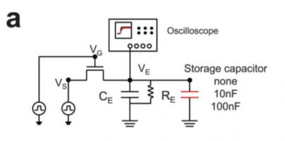
AM-(TFT-)EWOD
Article on AM-(TFT-)EWOD
Patents
1 Toward active-matrix lab-on-a-chip: programmable electrofluidic control enabled by arrayed oxide thin film transistors†
Joo Hyon Noh, a Jiyong Noh, a Eric Kreit, b Jason Heikenfeld b and Philip D. Rack
2 Electrowetting: from basics to applications, Frieder Mugele 1,3 and Jean-Christophe Baret
3 Programmable large area digital microfluidic array with integrated droplet sensing for bioassays, B. Hadwen, a G. R. Broder, b D. Morganti, b A. Jacobs, a C. Brown, a J. R. Hector, a Y. Kubota c and H. Morgan* b
