Difference between revisions of "Elektrowetting"
(→Intense fluxing (hacking session)) |
|||
| Line 108: | Line 108: | ||
File:fluxel incubated.JPG|alt=We put the box in the do-it-yourself incubator.|The box goes in the incubator | File:fluxel incubated.JPG|alt=We put the box in the do-it-yourself incubator.|The box goes in the incubator | ||
File:fluxel one night stand.JPG|We monitor cell growth overnight | File:fluxel one night stand.JPG|We monitor cell growth overnight | ||
| − | File: | + | File:beta_galactosidase.JPG|alt=Beta-galactosidase.|β-galactosidase in action (modeled by Rüdiger) |
</gallery> | </gallery> | ||
Revision as of 00:47, 16 March 2015
Contents
Introduction
- Electrical charge of the surface changes the shape of water drops (before 1875)
- Electrowetting is the modification of the wetting properties of a surface by applying different electric fields (1981)
- "fluid transistor" for manipulating chemical and biological fluids (1980)
- Electrowetting on this dielectric-coated surface, EWOD (1993)
- Digital Microfluidic Circuits
What you need:
- insulating dielectric and hydrophobic layers
- immiscible fluids
- DC or RF power
- mass arrays of miniature interleaved electrodes (Indium tin oxide (ITO))
- digital control
- nano droplets
What you can do:
- move droplets in linear, circular and directed paths
- pump fluids
- mix fluids
- fill reservoirs
- move droplets over sensors or heaters
- control fluid flow electronically or optically
source: http://en.wikipedia.org/wiki/Electrowetting

Electrowetting_TFT [1]
DIY experiment
What you need:
- ribbon cable
- water, oil
- high voltage (how high? Amperage? will 80v do?)
What you can do:

DIY Designs

Miri PCB Electrode Design
Fluxology


FluxMux-Device
Based on two crosswise flat ribbon cable the FluxMux device is an easy way to create a digital microfluidic device. An array of power leds shines through the grid to make drops visible.
The control is multiplexed.
Flux Technologies
comming soon...
Bio Device

Surface Coating

Electronic Control


[1,2,3]
Visit to DropBot @ Helsinki University


== DigiFlux Shield ==file:///media/gaudi/CANON_DC/DCIM/124___03/IMG_7383.JPG

Layouting first prototype of DigiFlux with array of fluxels
Etching some prototype shields.

Spin-coating with PDMS and teflon

Intense fluxing (hacking session)
We met in gaudilabs to experiment on the fluxel device. We first learned how to control the device and how to apply the coating properly.
We tested two bio-applications on fluxel: (1) growing E. coli DH5 alpha JM109 cells and (2) enzymatic reaction of β-galactosidase with Xgal.
For the first experiment, we wanted to investigate the impact of the electrical field on the growth of the E. coli cells. The setup consisted of the fluxel device, the arduino control, a webcam, a box and a computer with adequate software. We first dispensed a 30 μL droplet containing the E. coli cells on the fluxel device, covered it with a special lid to delay evaporation and then, carefully, we confined the fluxel device, the arduino and the webcam in a box. We put the box in the incubator and turned the fluxel device on. The droplet was incubated at 37°C. We monitored overnight the droplet using the ImageJ software running on a computer placed on top of the incubator. The droplet completely dried after 150 minutes, with an evaporation speed of ≈ 0.2 μL/min. We also noticed a change in the electrode surface: the electrodes became darker on the sides, probably due to the coating base (made of saran wrap) deteriorating due to heat exposure in the incubator. The deterioration of the coating base led to the droplets leaking though and being in direct contact with the electrode, which probably caused the corrosion of the electrodes. Also, the obtained images were of too poor quality and did not allow to properly measure the impact of the electrical field on the cells. One possible solution is to have a white background underneath the droplet to enhance the visibility of the cells growth. We are thinking of testing on shinny mirror-like electrodes or with a non-transparent coating base.
For the second experiment, we investigated the impact of the electrical field on the biochemical reaction of the β-galactosidase protein with Xgal.
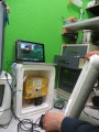
The box goes in the incubator
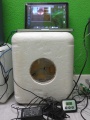
We monitor cell growth overnight
- Beta galactosidase.JPG
β-galactosidase in action (modeled by Rüdiger)


References
Fast Fabricating Electrowetting
Low Cost PCB Digital Microfluidic
Videos
On chip Sample preparation utilising EWOD Concept
DNA Lab on a Chip
Sandia Digital Microfluidic Hub
The Electrowetting Display
AM-(TFT-)EWOD
Article on AM-(TFT-)EWOD
Patents
1 Toward active-matrix lab-on-a-chip: programmable electrofluidic control enabled by arrayed oxide thin film transistors†
Joo Hyon Noh, a Jiyong Noh, a Eric Kreit, b Jason Heikenfeld b and Philip D. Rack
2 Electrowetting: from basics to applications, Frieder Mugele 1,3 and Jean-Christophe Baret
3 Programmable large area digital microfluidic array with integrated droplet sensing for bioassays, B. Hadwen, a G. R. Broder, b D. Morganti, b A. Jacobs, a C. Brown, a J. R. Hector, a Y. Kubota c and H. Morgan* b